- 您现在的位置:买卖IC网 > Sheet目录3890 > PIC18C858T-I/PT (Microchip Technology)IC MCU OTP 16KX16 CAN 80TQFP
PIC18CXX8
DS30475A-page 124
Advanced Information
2000 Microchip Technology Inc.
13.1
Timer3 Operation
Timer3 can operate in one of these modes:
As a timer
As a synchronous counter
As an asynchronous counter
The operating mode is determined by the clock select
bit, TMR3CS (T3CON register).
When TMR3CS = 0, Timer3 increments every instruc-
tion cycle. When TMR3CS = 1, Timer3 increments on
every rising edge of the Timer1 external clock input or
the Timer1 oscillator, if enabled.
When the Timer1 oscillator is enabled (T1OSCEN is
set), the RC1/T1OSI and RC0/T1OSO/T1CKI pins
become inputs. That is, the TRISC<1:0> value is
ignored.
Timer3 also has an internal “RESET input”. This
RESET can be generated by the CCP module
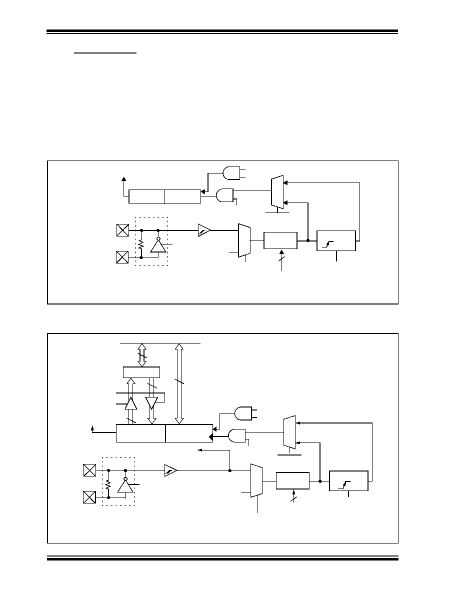
FIGURE 13-1: TIMER3 BLOCK DIAGRAM
FIGURE 13-2: TIMER3 BLOCK DIAGRAM CONFIGURED IN 16-BIT READ/WRITE MODE
TMR3H
TMR3L
T1OSC
T3SYNC
TMR3CS
T3CKPS1:T3CKPS0
SLEEP Input
T1OSCEN
Enable
Oscillator(1)
TMR3IF
Overflow
Interrupt
Fosc/4
Internal
Clock
TMR3ON
on/off
Prescaler
1, 2, 4, 8
Synchronize
det
1
0
1
Synchronized
Clock Input
2
T1OSO/
T1OSI
Flag bit
Note 1:
When enable bit T1OSCEN is cleared, the inverter and feedback resistor are turned off. This eliminates power drain.
T13CKI
CCP Special Trigger
T3CCPx
CLR
TMR3L
T1OSC
T3SYNC
TMR3CS
T3CKPS1:T3CKPS0
SLEEP Input
T1OSCEN
Enable
Oscillator(1)
FOSC/4
Internal
Clock
TMR3ON
On/Off
Prescaler
1, 2, 4, 8
Synchronize
det
1
0
1
Synchronized
Clock Input
2
T1OSO/
T1OSI
TMR3
T13CKI
CLR
CCP Special Trigger
T3CCPx
To Timer1 Clock Input
Note 1:
When the T1OSCEN bit is cleared, the inverter and feedback resistor are turned off. This eliminates power drain.
TMR3H
Data Bus<7:0>
8
TMR3H
8
Read TMR3L
Write TMR3L
TMR3IF Overflow
Interrupt Flag
bit
发布紧急采购,3分钟左右您将得到回复。
相关PDF资料
PIC18C658T-I/PT
IC MCU OTP 16KX16 CAN 64TQFP
PIC16LC717T-E/SS
IC MCU OTP 2KX14 A/D PWM 20SSOP
PIC16LC771T/SO
IC MCU OTP 4KX14 A/D PWM 20SOIC
PIC16LC771T-E/SO
IC MCU OTP 4KX14 A/D PWM 20SOIC
PIC16C771T-E/SO
IC MCU OTP 4KX14 A/D PWM 20SOIC
PIC16LC770T/SS
IC MCU OTP 2KX14 A/D PWM 20SSOP
PIC16LC717T-I/SO
IC MCU OTP 2KX14 A/D PWM 18SOIC
PIC16LC771T/SS
IC MCU OTP 4KX14 A/D PWM 20SSOP
相关代理商/技术参数
PIC18F1220-E/ML
功能描述:8位微控制器 -MCU 4KB 256 RAM 16 I/O RoHS:否 制造商:Silicon Labs 核心:8051 处理器系列:C8051F39x 数据总线宽度:8 bit 最大时钟频率:50 MHz 程序存储器大小:16 KB 数据 RAM 大小:1 KB 片上 ADC:Yes 工作电源电压:1.8 V to 3.6 V 工作温度范围:- 40 C to + 105 C 封装 / 箱体:QFN-20 安装风格:SMD/SMT
PIC18F1220-E/P
功能描述:8位微控制器 -MCU 4KB 256 RAM 16 I/O RoHS:否 制造商:Silicon Labs 核心:8051 处理器系列:C8051F39x 数据总线宽度:8 bit 最大时钟频率:50 MHz 程序存储器大小:16 KB 数据 RAM 大小:1 KB 片上 ADC:Yes 工作电源电压:1.8 V to 3.6 V 工作温度范围:- 40 C to + 105 C 封装 / 箱体:QFN-20 安装风格:SMD/SMT
PIC18F1220-E/SO
功能描述:8位微控制器 -MCU 4KB 256 RAM 16 I/O RoHS:否 制造商:Silicon Labs 核心:8051 处理器系列:C8051F39x 数据总线宽度:8 bit 最大时钟频率:50 MHz 程序存储器大小:16 KB 数据 RAM 大小:1 KB 片上 ADC:Yes 工作电源电压:1.8 V to 3.6 V 工作温度范围:- 40 C to + 105 C 封装 / 箱体:QFN-20 安装风格:SMD/SMT
PIC18F1220-E/SS
功能描述:8位微控制器 -MCU 4KB 256 RAM 16 I/O RoHS:否 制造商:Silicon Labs 核心:8051 处理器系列:C8051F39x 数据总线宽度:8 bit 最大时钟频率:50 MHz 程序存储器大小:16 KB 数据 RAM 大小:1 KB 片上 ADC:Yes 工作电源电压:1.8 V to 3.6 V 工作温度范围:- 40 C to + 105 C 封装 / 箱体:QFN-20 安装风格:SMD/SMT
PIC18F1220-H/ML
功能描述:8位微控制器 -MCU 4KB FL 256RAM 16 I/O RoHS:否 制造商:Silicon Labs 核心:8051 处理器系列:C8051F39x 数据总线宽度:8 bit 最大时钟频率:50 MHz 程序存储器大小:16 KB 数据 RAM 大小:1 KB 片上 ADC:Yes 工作电源电压:1.8 V to 3.6 V 工作温度范围:- 40 C to + 105 C 封装 / 箱体:QFN-20 安装风格:SMD/SMT
PIC18F1220-H/P
功能描述:8位微控制器 -MCU 4KB FL 256RAM 16 I/O RoHS:否 制造商:Silicon Labs 核心:8051 处理器系列:C8051F39x 数据总线宽度:8 bit 最大时钟频率:50 MHz 程序存储器大小:16 KB 数据 RAM 大小:1 KB 片上 ADC:Yes 工作电源电压:1.8 V to 3.6 V 工作温度范围:- 40 C to + 105 C 封装 / 箱体:QFN-20 安装风格:SMD/SMT
PIC18F1220-H/SO
功能描述:8位微控制器 -MCU 4KB FL 256RAM 16 I/O RoHS:否 制造商:Silicon Labs 核心:8051 处理器系列:C8051F39x 数据总线宽度:8 bit 最大时钟频率:50 MHz 程序存储器大小:16 KB 数据 RAM 大小:1 KB 片上 ADC:Yes 工作电源电压:1.8 V to 3.6 V 工作温度范围:- 40 C to + 105 C 封装 / 箱体:QFN-20 安装风格:SMD/SMT
PIC18F1220-H/SS
功能描述:8位微控制器 -MCU 4KB FL 256RAM 16 I/O RoHS:否 制造商:Silicon Labs 核心:8051 处理器系列:C8051F39x 数据总线宽度:8 bit 最大时钟频率:50 MHz 程序存储器大小:16 KB 数据 RAM 大小:1 KB 片上 ADC:Yes 工作电源电压:1.8 V to 3.6 V 工作温度范围:- 40 C to + 105 C 封装 / 箱体:QFN-20 安装风格:SMD/SMT